|
Semiconductor Wafer Positioning |
|
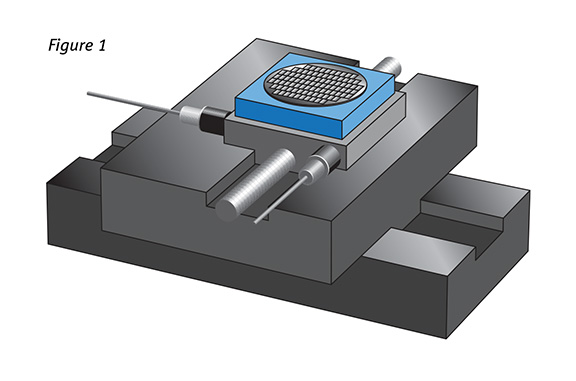
| GOAL Maintaining accuracy of the z-axis stage position — to subatomic levels — in photolithography processes for semiconductor wafer production.Maintaining high resolution and repeatability.Avoiding the undesirable effects — such as dither, hysteresis, and thermal drift — that occur in other stage-handling systems. SOLUTION In making critical z-height adjustments, the stage that holds the wafer must be in the exact focal plane of the energy source. Kaman’s system measures the position of the z-axis stage (see Figure 1) and provides an analog output — or an optional digital interface — to signal out-of-tolerance conditions. The sensor’s precision, repeatability, and resolution also allow the user to close the loop on stage positioning and focus. Result: Precise z-axis stage focusing and consistent line widths or higher level of process control.
THE KAMAN ADVANTAGE Non-contact. Using eddy current technology, each sensor can measure the position of the target without ever touching it. High resolution. The system can sense position change to one nanometer. Repeatability. The sensor allows highly-reproducible focusing of the z-axis stage. System versatility. The system is available with a wide range of sensor options Every application is unique. |
|